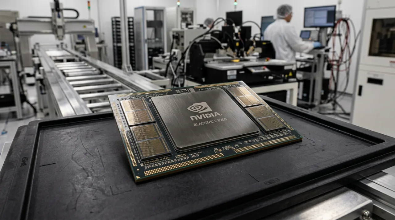
NVIDIA Blackwell GPUs entered volume production on TSMC’s 4NP process during the fourth quarter of 2026. The B200 and GB200 series use dual reticle-sized dies fabricated on the 4nm-class node, a customized variant of the 4N process employed for the prior Hopper generation. As of late October 2026, TSMC has increased wafer starts at its Arizona Fab 21 while continuing advanced CoWoS packaging in Taiwan.
NVIDIA Blackwell Output Gains From TSMC 4NP Maturity
Production of Blackwell wafers began in late 2025 and early 2026 after earlier delays from mid-2024 targets. Initial system deliveries occurred throughout 2025 and 2026, with output now accelerating as TSMC improves process control on the large 1,600 mm² class dies. Industry analysts note that reticle-limited dies remain yield-sensitive, yet TSMC’s established N5-family maturity supports continued scaling during the current quarter.
TSMC reported record quarterly profit in its Q3 2026 results and raised its full-year revenue growth outlook to approximately 44 percent in USD terms. The company guided Q4 2026 revenue between $52.3 billion and $54.3 billion, citing sustained AI and high-performance computing demand that exceeds available supply across leading-edge nodes. NVIDIA Blackwell production forms a significant portion of that demand.
On October 21, 2026, NVIDIA and its supply chain partners announced capacity expansions that include a 2.5 times increase in substrate capacity over three years, more than 300 percent growth in advanced packaging by the end of 2028, and doubled testing capacity by 2027. These steps directly support higher Blackwell throughput and address packaging constraints that previously limited overall output.
Supply Chain Expansions and Enterprise AI Accelerator Availability
Advanced CoWoS packaging and high-bandwidth memory supply continue to constrain final system volumes even as wafer production rises. TSMC’s Arizona facility now contributes to 4NP wafer output, yet high-end Blackwell variants still rely on Taiwan-based packaging lines. Partners such as Amkor and IBIDEN are expanding substrate and interposer capacity to relieve these bottlenecks.
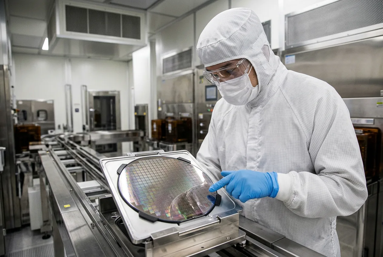
Enterprise customers deploying AI training clusters benefit from the improved availability. Larger memory configurations and higher interconnect bandwidth in the Blackwell architecture enable denser rack-scale systems compared with previous generations. Organizations planning 2027 infrastructure upgrades can now secure earlier delivery commitments as yield improvements translate into more completed systems per month.
TSMC’s Q3 2026 earnings highlighted that AI and HPC segments, including NVIDIA products, drive the majority of leading-edge revenue. The company expects similar dynamics to persist into 2027, when NVIDIA transitions toward the Rubin architecture on an N3P-class process. Continued 4NP ramp in the near term therefore serves as a bridge while packaging and memory ecosystems scale in parallel.
Forward Outlook for AI Chip Production Constraints
Next-quarter priorities center on sustaining 4NP yield gains and completing the announced substrate and packaging expansions. CoWoS capacity additions remain on the critical path, as does high-bandwidth memory allocation. NVIDIA has indicated that these elements will determine the pace of GB200 NVL rack deployments through the first half of 2027.
Enterprise buyers evaluating AI accelerator purchases should monitor TSMC quarterly guidance and NVIDIA supply-chain updates for signals on delivery lead times. The current trajectory points to steadily increasing Blackwell volumes through year-end 2026, provided packaging capacity keeps pace with wafer output.
Frequently asked questions
When did TSMC begin producing NVIDIA Blackwell wafers at Arizona Fab 21?
Wafer production at the Arizona facility reached an initial milestone around mid-October 2025, with ongoing output continuing into 2026 and increased volume in Q4 2026.
What packaging constraints affect NVIDIA Blackwell system deliveries?
Advanced CoWoS packaging and high-bandwidth memory supply remain the primary limits on final system volumes, even as wafer starts increase on the 4NP process.
How do the October 2026 capacity announcements support Blackwell production?
NVIDIA and partners committed to 2.5 times substrate capacity growth over three years, more than 300 percent advanced packaging expansion by end-2028, and doubled testing capacity by 2027.
What process node does NVIDIA Blackwell use?
The B200 and GB200 series employ dual reticle-sized dies on TSMC’s custom 4NP node, a 4nm-class variant of the 4N process previously used for Hopper GPUs.
By YasTech Editorial
Comments 3